- 您现在的位置:买卖IC网 > Sheet目录1994 > DS2404B (Maxim Integrated Products)IC ECONORAM TIMECHIP 5.5V 16SSOP
DS2404
18 of 29
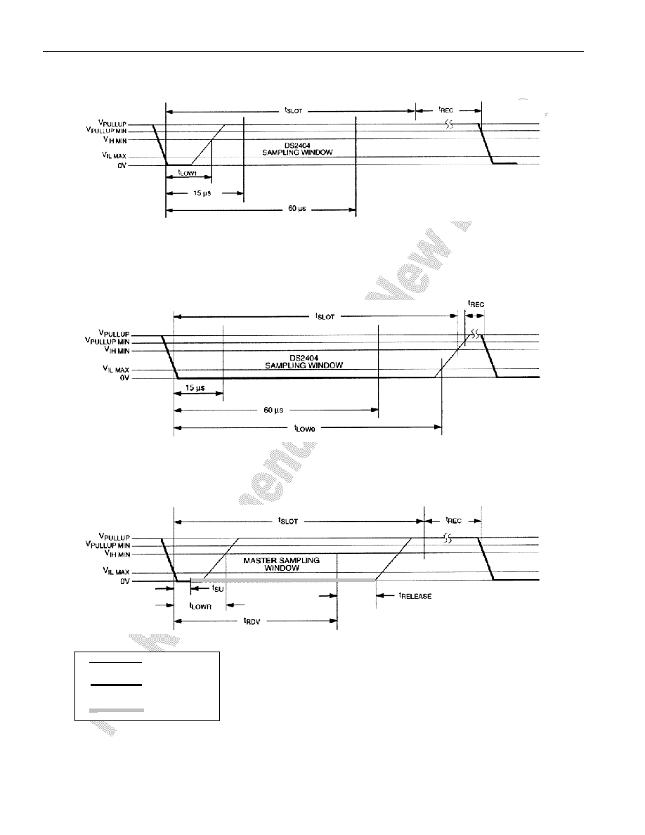
READ/WRITE TIMING DIAGRAM Figure 11
Write-one Time Slot
60
μs < tSLOT< 120μs
1
μs ≤ tLOW1< 15μs
1
μs ≤ tREC< ∞
Write-zero Time Slot
60
μs ≤ tLOW0< tSLOT< 120μs
1
μs ≤ tREC < ∞
Read-data Time Slot
60
μs ≤ tSLOT< 120μs
1
μs ≤ tLOWR< 15μs
0
≤ tRELEASE< 45μs
1
μs ≤ tREC< ∞
tRDV= 15μs
tSU< 1μs
RESISTOR
MASTER
DS2404
发布紧急采购,3分钟左右您将得到回复。
相关PDF资料
DS2415P+T&R
IC TIME CHIP 1-WIRE 6-TSOC
DS2417X/T&R
IC TIMECHIP W/INTRPT 1WIRE CSP
DS26502LN+
IC T1/E1/J1 64KCC ELEMENT 64LQFP
DS26503LN+
IC T1/E1/J1 BITS ELEMENT 64-LQFP
DS3105LN+
IC TIMING LINE CARD 64-LQFP
DS3106LN+
IC TIMING LINE CARD 64-LQFP
DS3231MZ+
IC RTC I2C 8SOIC
DS3231SN#T&R
IC RTC W/TCXO 16-SOIC
相关代理商/技术参数
DS2404B/T&R
制造商:Maxim Integrated Products 功能描述:ECONORAM/TIME, SSOP16-TRL (GENERIC) - Tape and Reel
DS2404B+
制造商:Maxim Integrated Products 功能描述:REAL TIME CLOCK SERL 512BYTE 16SSOP - Rail/Tube
DS2404B+T&R
制造商:Maxim Integrated Products 功能描述:REAL TIME CLOCK SERL 512BYTE 16SSOP - Tape and Reel
DS2404FP000
制造商:Thomas & Betts 功能描述:200A,CON,3P4W,MG,404,3P480V
DS2404FP000/DF2029
制造商:Thomas & Betts 功能描述:RS DS2404FP000/DF2029 200A,CON,3P4W
DS2404FP000/DF2032
制造商:Thomas & Betts 功能描述:200A,CON,3P4W,MG,404,3P480V,DF2032
DS2404FP00K
制造商:Thomas & Betts 功能描述:200A,CON,3P4W,MG,404,00K,3P480V
DS2404FPOOO/DF2029
制造商:Thomas & Betts 功能描述:RS DS2404FPOOO/DF2029 200A,CON,3P4W